| CPC H01L 23/53252 (2013.01) [H01L 23/53276 (2013.01); H10B 12/0335 (2023.02); H10B 12/315 (2023.02); H10B 12/482 (2023.02); H01L 21/76885 (2013.01)] | 17 Claims |
|
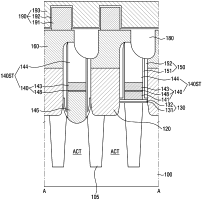
1. A semiconductor device comprising:
a substrate including an element isolation layer, the element isolation layer defining an active region;
a plurality of word lines traversing the active region in a first direction; and
a plurality of bit line structures on the substrate and connected to the active region, the plurality of bit line structures extending in a second direction different from the first direction,
wherein each of the plurality of bit line structures includes,
a ruthenium line wiring including a bottom surface and a top surface opposite to the bottom surface,
a lower graphene layer in contact with the bottom surface of the ruthenium line wiring and extending along the bottom surface of the ruthenium line wiring, and
a wiring line capping layer extending along the top surface of the ruthenium line wiring, wherein at least one of the plurality of bit line structures includes a sidewall graphene layer extending along a sidewall of the ruthenium line wiring and a sidewall of a first line wiring between the lower graphene layer and the substrate.
|