| CPC H01L 23/5283 (2013.01) [H01L 21/823871 (2013.01); H01L 23/528 (2013.01); H01L 23/5286 (2013.01); H01L 23/5386 (2013.01); H01L 27/0207 (2013.01); H01L 21/823475 (2013.01); H01L 27/11807 (2013.01); H01L 2027/11862 (2013.01); H01L 2027/11875 (2013.01); H01L 2027/11888 (2013.01)] | 8 Claims |
|
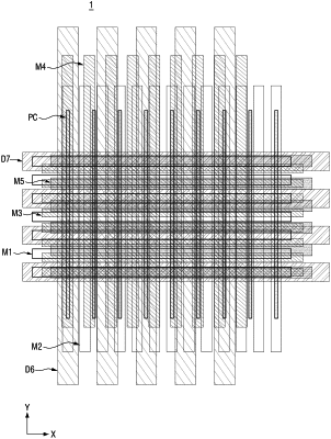
1. A method of designing a semiconductor device, the method comprising:
performing a simulation a number of times, the simulation including,
holding a gate pitch of a plurality of gate wiring patterns constant,
varying a first pitch of first wiring patterns of a plurality of first-direction wiring patterns that extend in a first direction,
varying a second pitch of second wiring patterns of the plurality of first-direction wiring patterns that extend in the first direction, and
varying a third pitch of third wiring patterns of the plurality of first-direction wiring patterns that extend in the first direction;
for each of the number of times, calculating a calculated least common multiple of the gate pitch, the first pitch, the second pitch, and the third pitch;
determining a determined least common multiple from among the calculated least common multiples; and
designing a plurality of layers based on the determined least common multiple.
|
|
6. A method of fabricating a semiconductor device, the method including:
performing a high-level design of the semiconductor device to generate a netlist of the semiconductor device;
designing a plurality of first-direction layouts of the semiconductor device based on the netlist;
performing optical proximity corrections on the plurality of first-direction layouts;
generating a plurality of photomasks based on the optical proximity correction; and
fabricating the semiconductor device based on the plurality of photomasks, wherein
the designing the plurality of first-direction layouts includes repeating a simulation a number of times, the simulation including,
holding a first pitch of a first one of the plurality of first-direction layouts constant,
varying other pitches of other ones of the plurality of first-direction layouts, and
calculating a least common multiple of the first pitch and each of the other pitches.
|