US 11,854,975 B2
Three-dimensional semiconductor device
Sung-Hun Lee, Yongin-si (KR); Seokjung Yun, Iksan-si (KR); Chang-Sup Lee, Hwaseong-si (KR); Seong Soon Cho, Suwon-si (KR); and Jeehoon Han, Hwaseong-si (KR)
Assigned to Samsung Electronics Co., Ltd., Suwon-si (KR)
Filed by Samsung Electronics Co., Ltd., Suwon-si (KR)
Filed on Aug. 27, 2021, as Appl. No. 17/459,406.
Application 16/247,712 is a division of application No. 15/350,305, filed on Nov. 14, 2016, granted, now 10,211,154, issued on Feb. 19, 2019.
Application 17/459,406 is a continuation of application No. 16/853,850, filed on Apr. 21, 2020, granted, now 11,107,765.
Application 16/853,850 is a continuation of application No. 16/247,712, filed on Jan. 15, 2019, abandoned.
Claims priority of application No. 10-2015-0182062 (KR), filed on Dec. 18, 2015.
Prior Publication US 2021/0391260 A1, Dec. 16, 2021
Int. Cl. H01L 23/528 (2006.01); H10B 41/20 (2023.01); H10B 41/27 (2023.01); H10B 43/10 (2023.01); H10B 43/20 (2023.01); H10B 43/27 (2023.01); H10B 43/35 (2023.01); H10B 43/50 (2023.01); H01L 21/768 (2006.01); H01L 23/522 (2006.01)
CPC H01L 23/5283 (2013.01) [H01L 21/76816 (2013.01); H01L 21/76877 (2013.01); H01L 23/5226 (2013.01); H10B 41/20 (2023.02); H10B 41/27 (2023.02); H10B 43/10 (2023.02); H10B 43/20 (2023.02); H10B 43/27 (2023.02); H10B 43/35 (2023.02); H10B 43/50 (2023.02)] 20 Claims
OG exemplary drawing
 
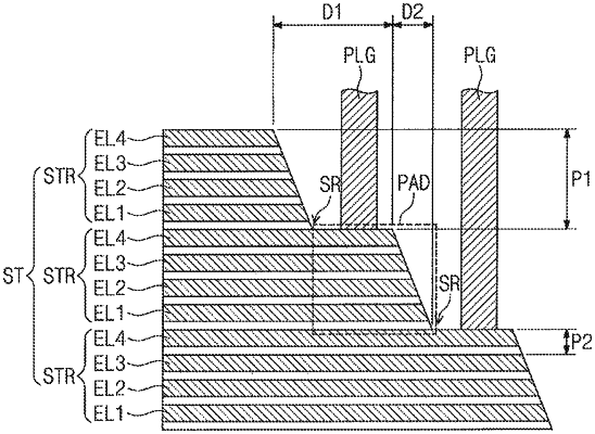
1. A semiconductor device comprising:
a substrate including a cell array region and a connection region; and
a stack structure including a first stack and a second stack on the first stack, each of the first and second stacks including at least three electrodes vertically stacked,
wherein the first stack has a first length in a first direction, the second stack has a second length in the first direction, and the second length is shorter than the first length, and
wherein each of the first and second stacks has a sloped sidewall defined by sidewalls of the at least three electrodes.