| CPC H01L 23/5283 (2013.01) [H01L 21/76804 (2013.01); H01L 23/5226 (2013.01); H10B 41/27 (2023.02); H10B 43/27 (2023.02)] | 7 Claims |
|
1. A semiconductor storage device comprising:
a substrate;
a plurality of conductive layers arranged in a first direction intersecting with a surface of the substrate;
a first insulating layer extending in the first direction;
a first semiconductor layer provided between the plurality of conductive layers and the first insulating layer; and
a gate insulating film provided between the plurality of conductive layers and the first semiconductor layer,
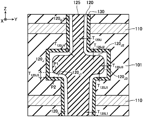
wherein a cross-section, extending in the first direction and a second direction intersecting with the first direction, in part includes a first one and a second one of the plurality of conductive layers that are adjacent to each other in the first direction, the first insulating layer, the first semiconductor layer, and the gate insulating film,
the first insulating layer includes:
a first insulating portion having a first width in the second direction, and
a second insulating portion that has a second width smaller than the first width in the second direction, and is separated from the first insulating portion in the first direction, and
the first semiconductor layer includes a first region provided between the first insulating portion and the first conductive layer, a second region provided between the second insulating portion and the second conductive layer, and a third region provided between the first region and the second region,
the third region includes a fourth region extending in the second direction, a fifth region provided between the first region and the fourth region, a sixth region provided between the second region and the fourth region, and a seventh region provided between the fifth region and the first region and extending in the first direction,
the first region of the first semiconductor layer has a first thickness from a surface on a side of the first insulating layer to the gate insulating film,
the second region of the first semiconductor layer has a second thickness from a surface on the side of the first insulating layer to the gate insulating film,
the seventh region of the first semiconductor layer has a third thickness from a surface on the side of the first insulating layer to the gate insulating film,
a surface in the fifth region on the side of the first insulating layer includes a region with a shortest distance to the gate insulating film larger than the first thickness, the second thickness, and the third thickness, and
a shortest distance to the gate insulating film from a surface in the sixth region on the side of the first insulating layer is larger than the first thickness minus 2 nm and is larger than the second thickness minus 2 nm.
|