| CPC H01L 23/528 (2013.01) [G06F 30/392 (2020.01); H01L 21/823807 (2013.01); H01L 21/823814 (2013.01); H01L 21/823871 (2013.01); H01L 21/823878 (2013.01); H01L 27/092 (2013.01); H10B 10/12 (2023.02)] | 20 Claims |
|
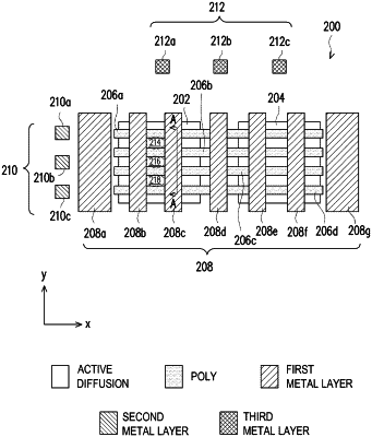
1. A combination circuit, comprising:
a set of cascading transistors that include a first internal node and a second internal node formed in an active region, the active region including at least one of a p-type well or an n-type well; and
a stack of conductive layers disposed over the active region and the set of cascading transistors, wherein each conductive layer in the stack of conductive layers comprises a plurality of conductive stripes and the first and the second internal nodes are not connected a common conductive stripe in the stack of conductive layers, the common conductive stripe comprising a single conductive stripe in the stack of conductive layers.
|