| CPC H01L 23/5226 (2013.01) [H01L 21/76802 (2013.01); H01L 21/76877 (2013.01); H01L 23/528 (2013.01); H01L 23/532 (2013.01)] | 20 Claims |
|
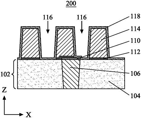
1. An interconnection structure, comprising:
a dielectric layer;
a first conductive feature disposed in the dielectric layer;
a hard mask layer disposed on the first conductive feature;
a conductive layer comprising a first portion and a second portion, wherein the first portion of the conductive layer is disposed over at least a first portion of the hard mask layer, and the second portion of the conductive layer is disposed over the dielectric layer, and wherein the hard mask layer and the conductive layer are formed by different materials;
a capping layer disposed on the dielectric layer and the conductive layer;
a dielectric fill disposed over the capping layer between the first portion and the second portion of the conductive layer;
an etch stop layer disposed over the dielectric fill and the conductive layer;
a dielectric material disposed over the etch stop layer; and
a second conductive feature disposed in the dielectric material over the first portion of the conductive layer.
|