| CPC H01L 23/49596 (2013.01) [H01L 23/3107 (2013.01); H01L 23/49503 (2013.01); H01L 23/49541 (2013.01); H01L 24/49 (2013.01); H01L 25/18 (2013.01); H01L 21/565 (2013.01); H01L 24/45 (2013.01); H01L 24/48 (2013.01); H01L 2224/05554 (2013.01); H01L 2224/45144 (2013.01); H01L 2224/45147 (2013.01); H01L 2224/48247 (2013.01); H01L 2224/4917 (2013.01); H01L 2224/49052 (2013.01); H01L 2224/49171 (2013.01); H01L 2924/07811 (2013.01); H01L 2924/14 (2013.01); H01L 2924/1461 (2013.01); H01L 2924/181 (2013.01); H01L 2924/3025 (2013.01); H01L 2924/37001 (2013.01); H01L 2924/3701 (2013.01)] | 4 Claims |
|
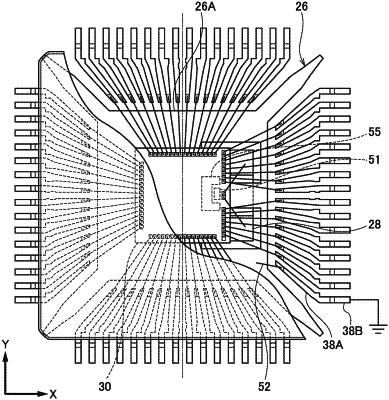
1. A semiconductor device comprising:
an oscillator comprising a plurality of external terminals that are disposed on a first face of the oscillator and that are separated from each other by a specific distance along a first direction on the first face;
an integrated circuit comprising a first region formed with a plurality of first electrode pads and a second region formed with a plurality of second electrode pads along one side on a first face of the integrated circuit, a distance between the first region and the second region in the first direction being narrower than a distance between the plurality of external terminals;
a lead frame comprising a die pad on which the oscillator and the integrated circuit are mounted and a plurality of leads that are formed along one side on the first face of the integrated circuit and that are electrically connected with the integrated circuit, the oscillator being mounted on the die pad such that the plurality of external terminals are sandwiched between the plurality of first electrode pads and the plurality of leads in a plan view;
a bonding wire that connects one of the plurality of external terminals to one of the plurality of first electrode pads;
a first circuit that is connected to the plurality of external terminals of the oscillator via the plurality of first electrode pads; and
a second circuit that is formed closer to an inner part of the integrated circuit than the first circuit, the first circuit being at least partly disposed in an opening in the second circuit, the second circuit being connected to the plurality of second electrode pads.
|