| CPC H01L 23/49575 (2013.01) [H01L 24/48 (2013.01); H03F 3/45475 (2013.01); H01L 2224/48247 (2013.01)] | 4 Claims |
|
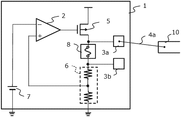
1. A semiconductor device, comprising:
an operational amplifier configured to receive a reference voltage from a reference voltage generation circuit and a feedback voltage from a feedback resistor;
an output transistor to be controlled by an output signal of the operational amplifier;
a first pad which is connected to an output terminal of the output transistor, and is to be selectively connected to a lead frame pad by a first bonding wire;
a second pad to be selectively connected to the lead frame pad by a second bonding wire;
a connection switching element provided between the first pad and the second pad; and
the feedback resistor connected to the second pad and the connection switching element,
wherein, the connection switching element interrupts connection between the first pad and the second pad in a case that the second pad is connected to the lead frame pad by the second bonding wire.
|