| CPC H01L 23/4952 (2013.01) [H01L 23/31 (2013.01); H01L 23/5384 (2013.01); H01L 23/5386 (2013.01); H01L 24/14 (2013.01); H01L 25/0657 (2013.01)] | 17 Claims |

|
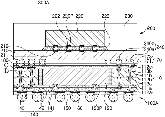
1. A semiconductor package comprising:
a first semiconductor package including:
a first package substrate including a redistribution layer,
a first semiconductor chip disposed on the first package substrate and electrically connected to the redistribution layer,
a molded member disposed on the first package substrate and covering the first package substrate and the first semiconductor chip,
a wiring structure disposed on the molded member and having an upper surface on which a plurality of upper pads are arranged, and
a frame disposed between the first package substrate and the wiring structure, having a through-hole in which the first semiconductor chip is disposed, the frame electrically connecting the redistribution layer and the plurality of upper pads;
a second semiconductor package disposed on the first semiconductor package, and including:
a second package substrate having a lower surface on which a plurality of lower redistribution pads are arranged, and
a second semiconductor chip disposed on the second package substrate and electrically connected to the plurality of lower redistribution pads; and
a plurality of connection bumps electrically connecting the plurality of upper pads and the plurality of lower redistribution pads,
wherein upper pads among the plurality of upper pads that are formed vertically under the second semiconductor package include a first upper pad adjacent to a corner of the upper surface of the wiring structure, and a second upper pad closer to a center of the upper surface of the wiring structure than the first upper pad,
the plurality of connection bumps include a first connection bump disposed in a position corresponding to the first upper pad and a second connection bump disposed in a position corresponding to the second upper pad,
a first width of the first upper pad is wider than a second width of the second upper pad,
a maximum width of the first connection bump is wider than a maximum width of the second connection bump,
a maximum thickness of the first connection bump in a vertical direction is less than a maximum thickness of the second connection bump in the vertical direction, and
the wiring structure further includes a contact layer disposed on the first upper pad between the first upper pad and the first connection bump.
|