| CPC H01L 23/485 (2013.01) [H01L 21/563 (2013.01); H01L 23/49838 (2013.01); H01L 24/17 (2013.01); H01L 25/0655 (2013.01); H01L 25/0657 (2013.01); H01L 25/18 (2013.01); H01L 2224/12105 (2013.01); H01L 2224/131 (2013.01); H01L 2224/13147 (2013.01); H01L 2224/16145 (2013.01); H01L 2224/16225 (2013.01); H01L 2224/1703 (2013.01); H01L 2224/17505 (2013.01); H01L 2224/26175 (2013.01); H01L 2224/2919 (2013.01); H01L 2224/32058 (2013.01); H01L 2224/32145 (2013.01); H01L 2224/32225 (2013.01); H01L 2224/73204 (2013.01); H01L 2224/81203 (2013.01); H01L 2225/06513 (2013.01); H01L 2225/06517 (2013.01); H01L 2225/06568 (2013.01); H01L 2924/12042 (2013.01); H01L 2924/15192 (2013.01); H01L 2924/15311 (2013.01); H01L 2924/181 (2013.01)] | 28 Claims |
|
1. A semiconductor package, comprising:
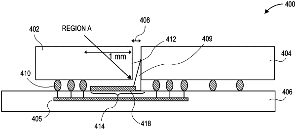
first and second adjacent semiconductor dies separated by a spacing;
a silicon interposer structure disposed below and electrically coupling the first and second semiconductor dies, wherein the first semiconductor die is coupled to the silicon interposer structure by a plurality of conductive bumps;
an organic package substrate disposed below and electrically coupled to the silicon interposer structure, the organic package substrate comprising a plurality of routing layers therein;
a metal barrier structure disposed between the first semiconductor die and the silicon interposer structure and at least partially underneath the first semiconductor die, wherein the metal barrier structure is spaced apart from the plurality of conductive bumps coupling the first semiconductor die to the silicon interposer structure; and
an underfill material layer in contact with the second semiconductor die and with the metal barrier structure, but not in contact with the first semiconductor die, at least a portion of the underfill material layer overlapping the metal barrier structure in a plan view.
|