| CPC H01L 23/481 (2013.01) [H01L 24/11 (2013.01); H01L 24/14 (2013.01); H01L 25/0652 (2013.01); H10B 12/01 (2023.02); H10B 12/30 (2023.02); H01L 2224/17104 (2013.01)] | 4 Claims |
|
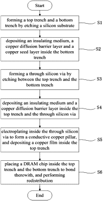
1. A three-dimensional integrated system for DRAM chips, comprising:
a top trench, a bottom trench and a through silicon via that penetrate through a silicon substrate (200), wherein the through silicon via connects the top trench and the bottom trench;
a first insulating medium (201), a first copper diffusion barrier layer (202) and a copper seed layer (203), wherein the first insulating medium (201) covers the bottom trench and is discontinuous at the bottom of the through silicon via; the first copper diffusion barrier layer (202) is formed on the first insulating medium (201); the copper seed layer (203) covers the first copper diffusion barrier layer (202), and appears a continuous film; the first copper diffusion barrier layer (202) and the copper seed layer (203) are disconnected at a connection area between adjacent bottom trenches to achieve insulation;
a second insulating medium (204), a second copper diffusion barrier layer (205), a copper film (207) and a conductive copper pillar (206), wherein the second insulating medium (204) covers the top trench and the through silicon via, and is discontinuous at the bottom of the through silicon via; the second copper diffusion barrier layer (205) covers the second insulating medium (204); the copper film (207) covers the second copper diffusion barrier layer (205) within the top trench and appears a continuous film; the conductive copper pillar (206) covers the second copper diffusion barrier layer (205) on the sidewall of the through silicon via, and completely fills the through silicon via, the top of the conductive copper pillar (206) is in contact with the copper film (207), and the bottom of the conductive copper pillar (206) is in contact with the copper seed layer (203); the second copper diffusion barrier layer (205) and the copper film (207) is disconnected at a connection area of adjacent top trenches to achieve insulation;
a DRAM chip (208), contact bumps (209), a filler (210) and a redistribution layer (211), wherein the DRAM chip (208) is bonded to the copper seed layer (203) and the copper film (207) respectively through the contact bumps (209); the filler (210) fills the gaps between the DRAM chip (208) and the top trench as well as between the DRAM chip (208) and the bottom trench; the redistribution layer (211) covers the top and the bottom of the three-dimensional integrated system.
|