| CPC H01L 23/3121 (2013.01) [H01L 24/19 (2013.01); H01L 24/20 (2013.01); H01L 24/24 (2013.01); H01L 24/73 (2013.01); H01L 24/92 (2013.01); H01L 24/97 (2013.01); H01L 24/02 (2013.01); H01L 24/16 (2013.01); H01L 24/32 (2013.01); H01L 2224/0233 (2013.01); H01L 2224/16227 (2013.01); H01L 2224/19 (2013.01); H01L 2224/221 (2013.01); H01L 2224/244 (2013.01); H01L 2224/24137 (2013.01); H01L 2224/24155 (2013.01); H01L 2224/32137 (2013.01); H01L 2224/32155 (2013.01); H01L 2224/32225 (2013.01); H01L 2224/73204 (2013.01); H01L 2224/73209 (2013.01); H01L 2224/73217 (2013.01); H01L 2224/73267 (2013.01); H01L 2224/9211 (2013.01); H01L 2224/92125 (2013.01); H01L 2224/92135 (2013.01); H01L 2924/19041 (2013.01); H01L 2924/19042 (2013.01); H01L 2924/19043 (2013.01); H01L 2924/19104 (2013.01)] | 24 Claims |
|
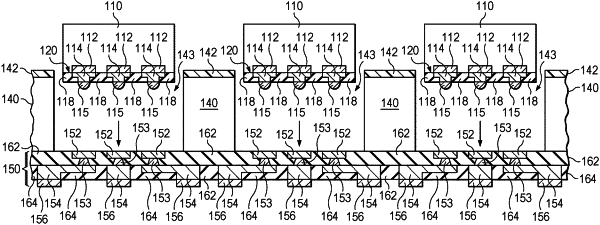
1. A semiconductor package, comprising:
a semiconductor substrate including a cavity;
a redistribution layer on a first side of the semiconductor substrate, the redistribution layer
forming die contacts within the cavity on a first side of the semiconductor substrate and a set of terminals of the semiconductor package on a second side of the semiconductor substrate,
wherein the redistribution layer electrically connects one or more of the die contacts to the set of terminals; and
a semiconductor die including die terminals within the cavity with the die terminals electrically coupled to the die contacts within the cavity.
|