| CPC H01L 22/32 (2013.01) [G01R 31/2644 (2013.01); H01L 21/565 (2013.01); H01L 21/78 (2013.01); H01L 21/82 (2013.01); H01L 22/12 (2013.01); H01L 23/562 (2013.01); H01L 23/564 (2013.01); H01L 23/585 (2013.01); H01L 24/13 (2013.01); H01L 2224/13024 (2013.01)] | 20 Claims |
|
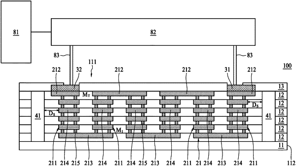
1. A method for detecting defects in a semiconductor device, comprising:
singulating a die having a substrate including a circuit region and an outer border, a plurality of detecting devices disposed over the substrate and located between the circuit region and the outer border, a first probe pad and a second probe pad electrically connected to two ends of each detecting device, and a seal ring located between the outer border of the die and the detecting devices;
providing a first bump and a second bump respectively on the first probe pad and the second probe pad;
probing the first probe pad and the second probe pad through the first bumps and the second bump to determine a connection status of the detecting devices; and
recognizing a defect when the connection status of the detecting devices indicates an open circuit.
|