| CPC H01L 22/32 (2013.01) [H01L 23/3128 (2013.01); H01L 24/05 (2013.01); H01L 24/24 (2013.01); H01L 2224/022 (2013.01); H01L 2224/24226 (2013.01)] | 20 Claims |
|
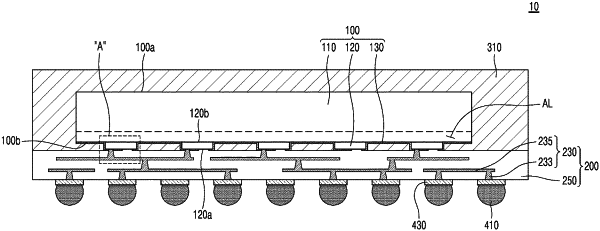
1. A semiconductor package comprising:
a chip pad of a semiconductor chip, the chip pad comprising a connection portion and a test portion in a first surface of the chip pad;
a barrier layer covering the chip pad, the barrier layer defining a first opening and a second opening that is separate from the first opening, the first opening exposing the connection portion of the chip pad, and the second opening exposing the test portion of the chip pad; and
a redistribution structure connected to the chip pad and comprising a redistribution dielectric layer, a redistribution via pattern, and a redistribution line pattern, the redistribution dielectric layer covering the chip pad and the barrier layer, the redistribution via pattern passing through at least a portion of the redistribution dielectric layer in a vertical direction, filling the first opening and being in contact with the connection portion of the chip pad, and the redistribution line pattern extending in a horizontal direction between, along the vertical direction, portions of the redistribution dielectric layer, and being connected to the redistribution via pattern.
|