US 11,854,909 B2
Semiconductor structure and method for manufacturing thereof
Man-Ho Kwan, Kowloon (HK); Fu-Wei Yao, Hsinchu (TW); Ru-Yi Su, Yunlin County (TW); Chun Lin Tsai, Hsin-Chu (TW); and Alexander Kalnitsky, San Francisco, CA (US)
Assigned to TAIWAN SEMICONDUCTOR MANUFACTURING COMPANY LTD., Hsinchu (TW)
Filed by TAIWAN SEMICONDUCTOR MANUFACTURING COMPANY LTD., Hsinchu (TW)
Filed on Jul. 26, 2022, as Appl. No. 17/814,870.
Application 17/814,870 is a division of application No. 16/433,775, filed on Jun. 6, 2019, granted, now 11,430,702.
Application 15/460,894 is a division of application No. 14/928,623, filed on Oct. 30, 2015, granted, now 9,627,275, issued on Apr. 18, 2017.
Application 16/433,775 is a continuation of application No. 15/460,894, filed on Mar. 16, 2017, granted, now 10,319,644, issued on Jun. 11, 2019.
Prior Publication US 2022/0359295 A1, Nov. 10, 2022
Int. Cl. H01L 21/8252 (2006.01); H01L 21/02 (2006.01); H01L 21/265 (2006.01); H01L 21/768 (2006.01); H01L 21/8258 (2006.01); H01L 29/06 (2006.01); H01L 29/205 (2006.01); H01L 23/535 (2006.01); H01L 21/761 (2006.01); H01L 27/06 (2006.01); H01L 29/16 (2006.01); H01L 29/778 (2006.01); H01L 29/78 (2006.01); H01L 29/866 (2006.01); H01L 29/20 (2006.01)
CPC H01L 21/8252 (2013.01) [H01L 21/0254 (2013.01); H01L 21/02381 (2013.01); H01L 21/02543 (2013.01); H01L 21/02546 (2013.01); H01L 21/02549 (2013.01); H01L 21/26546 (2013.01); H01L 21/761 (2013.01); H01L 21/76898 (2013.01); H01L 21/8258 (2013.01); H01L 27/0605 (2013.01); H01L 27/0688 (2013.01); H01L 29/0646 (2013.01); H01L 29/16 (2013.01); H01L 29/205 (2013.01); H01L 23/535 (2013.01); H01L 29/2003 (2013.01); H01L 29/7786 (2013.01); H01L 29/78 (2013.01); H01L 29/866 (2013.01)] 20 Claims
OG exemplary drawing
 
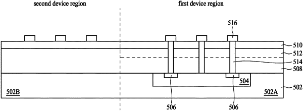
9. A method for manufacturing a semiconductor structure, comprising:
providing a silicon substrate having a first device region and a second device region;
forming a III-V layer on the silicon substrate laterally covering the first device region and the second device region;
forming an ion implanted region in the III-V layer over the first device region, and the ion implanted region includes negatively-charged ions; and
forming an interconnect penetrating the ion implanted region.