| CPC H01L 21/823431 (2013.01) [H01L 21/0206 (2013.01); H01L 21/0217 (2013.01); H01L 21/02068 (2013.01); H01L 21/02164 (2013.01); H01L 21/02238 (2013.01); H01L 21/02532 (2013.01); H01L 21/324 (2013.01); H01L 21/823481 (2013.01); H01L 21/823807 (2013.01); H01L 21/823821 (2013.01); H01L 21/823878 (2013.01); H01L 27/0924 (2013.01); H01L 29/0653 (2013.01); H01L 29/1037 (2013.01); H01L 29/165 (2013.01); H01L 29/66795 (2013.01); H01L 29/785 (2013.01)] | 20 Claims |
|
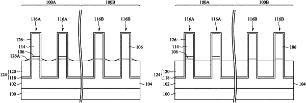
16. A method of manufacturing a semiconductor device, the method comprising:
forming a liner on exposed surfaces of a trench, the trench being between a first fin and a second fin;
depositing an insulation material in the trench;
forming a cap layer over the first fin, the second fin, the liner, and the insulation material, wherein the cap layer comprises:
a crystalline silicon cap portion, the crystalline silicon cap portion covering the first fin and the second fin; and
an amorphous silicon portion, the amorphous silicon portion being over respective upper surfaces of the liner and the insulation material; and
removing the amorphous silicon portion with an HCl etch.
|