| CPC H01L 21/823431 (2013.01) [H01L 21/823418 (2013.01); H01L 21/823468 (2013.01); H01L 21/823475 (2013.01); H01L 21/823481 (2013.01); H01L 21/823814 (2013.01); H01L 27/0886 (2013.01); H01L 29/0649 (2013.01); H01L 29/0653 (2013.01); H01L 29/161 (2013.01); H01L 29/165 (2013.01); H01L 29/1608 (2013.01); H01L 29/41783 (2013.01); H01L 29/41791 (2013.01); H01L 29/42364 (2013.01); H01L 29/518 (2013.01); H01L 29/665 (2013.01); H01L 29/6653 (2013.01); H01L 29/6656 (2013.01); H01L 29/66545 (2013.01); H01L 29/66636 (2013.01); H01L 29/66795 (2013.01); H01L 29/785 (2013.01); H01L 29/7842 (2013.01); H01L 29/7848 (2013.01); H01L 29/7851 (2013.01); H01L 29/7853 (2013.01); H01L 29/7854 (2013.01); H01L 2029/7858 (2013.01)] | 20 Claims |
|
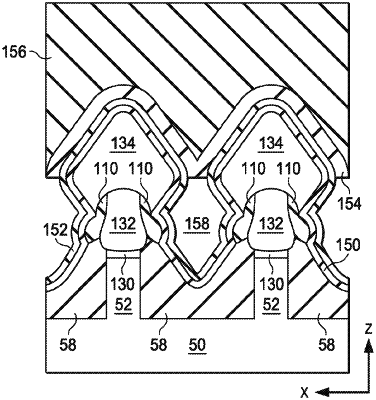
1. A field effect transistor (FinFET) device, comprising:
a semiconductor substrate;
a first epitaxial region over and separated from the semiconductor substrate, the first epitaxial region being located in a source/drain region of the FinFET device;
a shallow trench isolation (STI) region around the first epitaxial region, wherein the shallow trench isolation (STI) region directly contacts a bottom surface of the first epitaxial region and directly contacts side surfaces of the first epitaxial region that are disposed above the bottom surface of the first epitaxial region; and
a second epitaxial region formed on the first epitaxial region in the source/drain region.
|