| CPC H01L 21/823418 (2013.01) [H01L 21/823412 (2013.01); H01L 21/823431 (2013.01); H01L 27/088 (2013.01); H01L 29/0665 (2013.01); H01L 29/42392 (2013.01); H01L 29/66545 (2013.01); H01L 29/785 (2013.01); H01L 29/7855 (2013.01); H01L 29/78696 (2013.01)] | 20 Claims |
|
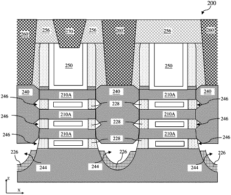
17. A method of forming a semiconductor device, comprising:
alternately forming first semiconductor layers and second semiconductor layers over a substrate, wherein the first semiconductor layers and the second semiconductor layers include different materials and are stacked up along a direction substantially perpendicular to a top surface of the substrate;
depositing a dielectric liner over a topmost first semiconductor layer of the first semiconductor layers;
after the depositing of the dielectric liner, forming dummy gate structures over channel regions of the first and second semiconductor layers;
removing a S/D region of the first and second semiconductor layers to form a source/drain (S/D) trench, such that the first semiconductor layers and the second semiconductor layers are truncated by the S/D trench and a recessed surface of the substrate is exposed in the S/D trench;
forming an isolation layer covering the recessed surface of the substrate exposed in the S/D trench; and
epitaxial growing semiconductor material between the truncated first semiconductor layers to form a bulk S/D feature,
wherein the forming the isolation layer covering the recessed surface of the substrate exposed in the S/D trench includes:
depositing a dielectric layer along sidewalls of the S/D trench and on the recessed surface of the substrate,
depositing an organic material over the dielectric layer,
etching back the organic material to form a buffer feature, wherein a top surface of the buffer feature is below a bottom surface of a lowermost second semiconductor layer,
removing a portion of the dielectric layer over the buffer feature to form the isolation layer, and
removing the buffer feature.
|