| CPC H01L 21/78 (2013.01) [H01L 21/0206 (2013.01); H01L 24/80 (2013.01); H01L 24/94 (2013.01); H01L 24/97 (2013.01); H01L 2224/80895 (2013.01); H01L 2224/80896 (2013.01); H01L 2224/94 (2013.01); H01L 2224/97 (2013.01)] | 20 Claims |
|
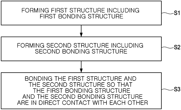
1. A method of manufacturing a semiconductor package, comprising:
forming a mask layer on a wafer, the wafer including a semiconductor substrate and an insulating layer;
forming a groove in the semiconductor substrate by performing a first laser grooving process;
expanding an opening of the mask layer opened by the first laser grooving process by performing a second laser grooving process;
exposing a portion of the insulating layer by removing a portion of the mask layer; and
cutting the semiconductor substrate while removing the portion of the insulating layer exposed during the exposing by performing a dicing process.
|