| CPC H01L 21/78 (2013.01) [H01L 21/268 (2013.01); H01L 21/304 (2013.01); H01L 21/6836 (2013.01); H01L 2221/68336 (2013.01)] | 17 Claims |
|
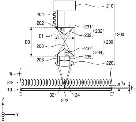
1. A laser apparatus, comprising:
a light source generating a laser beam;
an objective lens receiving the laser beam;
a first axicon lens between the objective lens and the light source; and
a second axicon lens between the first axicon lens and the objective lens,
wherein the first axicon lens and the second axicon lens include a first inclined surface and a second inclined surface, respectively, which are inclined at an inclination angle of 50° to 54° with respect to an optical axis of the laser beam, and
wherein the objective lens, the first axicon lens, and the second axicon lens are spaced apart from each other in a linear direction and the linear direction corresponds to the optical axis of the laser beam when the light source generates the laser beam,
wherein the objective lens has a numerical aperture of 0.8, and
wherein the inclination angle of the first inclined surface and the second inclined surface with respect to the optical axis are 51.3°.
|