| CPC H01L 21/76898 (2013.01) [H01L 21/288 (2013.01); H01L 21/2855 (2013.01); H01L 21/308 (2013.01); H01L 21/30625 (2013.01)] | 6 Claims |

|
1. A method of forming a through-silicon via structure, comprising:
applying and patterning a first resist film on a first side of a silicon substrate;
etching the silicon substrate through the patterned first resist film to form a hole in the first side;
plating a conductive material over the first side of the silicon substrate, the conductive material extending through the hole;
grinding or polishing the first side of the silicon substrate, wherein the grinding or polishing removes the conductive material disposed outside of the hole;
applying and patterning a second resist film on the first side of the silicon substrate;
etching the silicon substrate through the patterned second resist film to form a trench in the first side, the trench surrounding the hole having the conductive material extending therethrough;
laminating a dielectric film onto the first side of the silicon substrate, the lamination of the dielectric film causing a dielectric material of the dielectric film to fill the trench; and
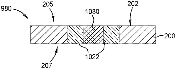
grinding or polishing the first side of the silicon substrate and a second side opposite the first side, wherein the grinding or polishing removes the dielectric film disposed outside of the trench, and wherein the grinding or polishing further exposes the conductive material and the dielectric material on the first side and the second side.
|