| CPC H01L 21/76897 (2013.01) [H01L 21/76816 (2013.01); H01L 21/76832 (2013.01); H01L 21/76837 (2013.01); H01L 21/76885 (2013.01); H01L 23/528 (2013.01); H01L 23/5226 (2013.01); H01L 21/7682 (2013.01)] | 25 Claims |
|
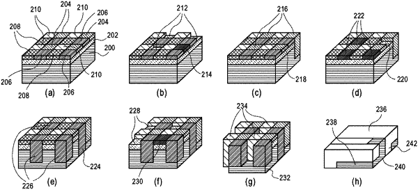
1. A method of fabricating a back end of line (BEOL) metallization layer for a semiconductor structure, the method comprising:
forming a metal layer above a substrate;
performing a first photobucket process to form one or more conductive vias in the metal layer;
performing a second photobucket process to form one or more cut locations in the metal layer;
performing a third photobucket process to form one or more conductive tabs in the metal layer; and
subtractively etching a plurality of metal lines in the metal layer, the plurality of metal lines coupled to the one or more conductive vias, coupled to the one or more conductive tabs, and having a continuity broken by the one or more cut locations.
|