| CPC H01L 21/76877 (2013.01) [H01L 21/561 (2013.01); H01L 21/563 (2013.01); H01L 21/565 (2013.01); H01L 21/6835 (2013.01); H01L 21/76802 (2013.01); H01L 23/3121 (2013.01); H01L 23/3135 (2013.01); H01L 23/3142 (2013.01); H01L 23/3157 (2013.01); H01L 23/481 (2013.01); H01L 24/19 (2013.01); H01L 24/20 (2013.01); H01L 24/97 (2013.01); H01L 25/0657 (2013.01); H01L 25/105 (2013.01); H01L 25/50 (2013.01); H01L 21/568 (2013.01); H01L 23/3128 (2013.01); H01L 24/17 (2013.01); H01L 24/48 (2013.01); H01L 24/49 (2013.01); H01L 24/73 (2013.01); H01L 24/83 (2013.01); H01L 24/92 (2013.01); H01L 2221/68359 (2013.01); H01L 2224/16113 (2013.01); H01L 2224/16227 (2013.01); H01L 2224/2919 (2013.01); H01L 2224/48091 (2013.01); H01L 2224/48106 (2013.01); H01L 2224/48229 (2013.01); H01L 2224/73267 (2013.01); H01L 2224/8385 (2013.01); H01L 2224/92244 (2013.01); H01L 2225/0651 (2013.01); H01L 2225/0652 (2013.01); H01L 2225/06517 (2013.01); H01L 2225/06548 (2013.01); H01L 2225/06568 (2013.01); H01L 2225/06572 (2013.01); H01L 2225/06586 (2013.01); H01L 2225/1035 (2013.01); H01L 2225/1058 (2013.01); H01L 2924/00014 (2013.01); H01L 2924/01013 (2013.01); H01L 2924/01022 (2013.01); H01L 2924/01028 (2013.01); H01L 2924/01029 (2013.01); H01L 2924/01074 (2013.01); H01L 2924/13091 (2013.01); H01L 2924/15311 (2013.01); H01L 2924/181 (2013.01); H01L 2924/18162 (2013.01)] | 20 Claims |
|
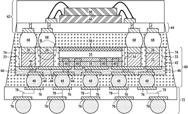
1. A method of manufacturing a semiconductor device, the method comprising:
providing a carrier;
forming a sacrificial layer on the carrier;
forming a through via over and in contact with the sacrificial layer;
disposing a die on the sacrificial layer, wherein the die has a plurality of metal pillars disposed at a side of the die facing away from the sacrificial layer;
forming a molding compound on the sacrificial layer to fill gaps between the die and the through via;
removing the carrier and sacrificial layer, wherein the sacrificial layer is removed concurrently with the removal of the carrier, thereby exposing one end of the through via and the molding compound; and
disposing a solder ball on the end of the through via.
|