US 11,854,869 B2
Methods of forming high aspect ratio features
Ken Tokashiki, Boise, ID (US); John A. Smythe, Boise, ID (US); and Gurtej S. Sandhu, Boise, ID (US)
Filed by Micron Technology, Inc., Boise, ID (US)
Filed on Jul. 7, 2022, as Appl. No. 17/811,285.
Application 17/811,285 is a continuation of application No. 17/155,770, filed on Jan. 22, 2021, granted, now 11,417,565.
Application 17/155,770 is a continuation of application No. 15/858,021, filed on Dec. 29, 2017, granted, now 10,903,109, issued on Jan. 26, 2021.
Prior Publication US 2022/0344200 A1, Oct. 27, 2022
This patent is subject to a terminal disclaimer.
Int. Cl. H01L 21/768 (2006.01); H01L 21/3065 (2006.01); H01L 21/762 (2006.01); H01L 21/311 (2006.01)
CPC H01L 21/76804 (2013.01) [H01L 21/30655 (2013.01); H01L 21/31116 (2013.01); H01L 21/76205 (2013.01); H01L 21/76816 (2013.01); H01L 21/76843 (2013.01); H01L 21/76831 (2013.01)] 24 Claims
OG exemplary drawing
 
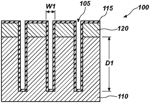
1. A method of forming high aspect ratio features, comprising:
forming high aspect ratio openings in a stack of dielectric materials at a temperature of less than about 0° C.;
forming an organic protective material at a temperature between about −100° C. and about −40° C. on sidewalls of the stack, the organic protective material formed by molecular layer deposition; and
forming features in the high aspect ratio openings, at least some of the features comprising high aspect ratio pillars.