| CPC H01L 21/76229 (2013.01) [H01L 21/02126 (2013.01); H01L 21/02164 (2013.01); H01L 21/02238 (2013.01); H01L 21/76237 (2013.01)] | 16 Claims |
|
1. A method of forming a semiconductor device, the method comprising:
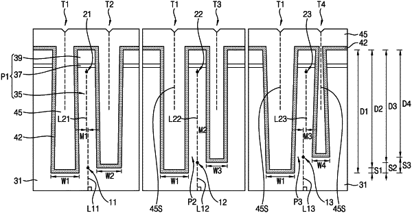
forming, on a substrate, a plurality of trenches defining a plurality of patterns, the plurality of trenches including a plurality of first trenches and a second trench adjacent one of the plurality of first trenches, the plurality of patterns including a first pattern between the second trench and the one of the plurality of first trenches, and the second trench having a different depth from the one of the plurality of first trenches adjacent thereto;
deforming the first pattern by forming a leaning control layer on side walls and bottoms of the plurality of trenches, wherein the first pattern is deformed to lean in a direction away from second trench and toward the one of the plurality of first trenches; and
forming a gap-fill insulating layer on the leaning control layer,
wherein the forming the leaning control layer comprises
forming a preliminary liner on the side walls and the bottoms of the plurality of trenches, and
oxidizing the preliminary liner using an oxidation process.
|