US 11,854,820 B2
Spacer etching process for integrated circuit design
Ru-Gun Liu, Hsinchu County (TW); Cheng-Hsiung Tsai, Miaoli County (TW); Chung-Ju Lee, Hsinchu (TW); Chih-Ming Lai, Hsinchu (TW); Chia-Ying Lee, New Taipei (TW); Jyu-Horng Shieh, Hsin-Chu (TW); Ken-Hsien Hsieh, Taipei (TW); Ming-Feng Shieh, Tainan County (TW); Shau-Lin Shue, Hsinchu (TW); Shih-Ming Chang, Hsin-Chu (TW); Tien-I Bao, Taoyuan County (TW); and Tsai-Sheng Gau, HsinChu (TW)
Assigned to TAIWAN SEMICONDUCTOR MANUFACTURING COMPANY, LTD., Hsinchu (TW)
Filed by Taiwan Semiconductor Manufacturing Company, Ltd., Hsin-Chu (TW)
Filed on May 22, 2020, as Appl. No. 16/882,063.
Application 16/882,063 is a division of application No. 15/357,203, filed on Nov. 21, 2016, granted, now 10,665,467.
Application 14/850,764 is a division of application No. 14/081,345, filed on Nov. 15, 2013, granted, now 9,153,478, issued on Jun. 10, 2015.
Application 15/357,203 is a continuation of application No. 14/850,764, filed on Sep. 10, 2015, granted, now 9,502,261.
Claims priority of provisional application 61/791,138, filed on Mar. 15, 2013.
Prior Publication US 2020/0286738 A1, Sep. 10, 2020
This patent is subject to a terminal disclaimer.
Int. Cl. H01L 21/308 (2006.01); H01L 21/033 (2006.01); H01L 21/311 (2006.01); H01L 21/768 (2006.01); H01L 21/02 (2006.01); H01L 21/027 (2006.01); H01L 21/3105 (2006.01); H01L 21/8234 (2006.01)
CPC H01L 21/3086 (2013.01) [H01L 21/0217 (2013.01); H01L 21/0276 (2013.01); H01L 21/02186 (2013.01); H01L 21/02282 (2013.01); H01L 21/0337 (2013.01); H01L 21/3081 (2013.01); H01L 21/31053 (2013.01); H01L 21/31055 (2013.01); H01L 21/31111 (2013.01); H01L 21/31144 (2013.01); H01L 21/76816 (2013.01); H01L 21/823431 (2013.01)] 20 Claims
OG exemplary drawing
 
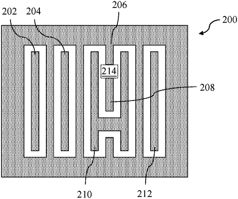
1. A method, comprising:
forming a first layer on a substrate;
forming a first plurality of trenches in the first layer by a first patterning process;
forming a second plurality of trenches in the first layer by a second patterning process, resulting in combined trench patterns in the first layer, wherein a first trench of the second plurality of trenches connects two trenches of the first plurality of trenches; and
forming dielectric spacer features on sidewalls of the combined trench patterns, wherein a first space between two opposing sidewalls of the first trench is completely filled by the dielectric spacer features and a second space between two opposing sidewalls of one of the two trenches is partially filled by the dielectric spacer features.