| CPC H01L 21/02057 (2013.01) [B08B 1/001 (2013.01); B08B 1/007 (2013.01); B08B 1/04 (2013.01); B08B 3/024 (2013.01); H01L 21/0206 (2013.01); H01L 21/304 (2013.01); H01L 21/6704 (2013.01); H01L 21/67051 (2013.01); H01L 21/68728 (2013.01)] | 20 Claims |
|
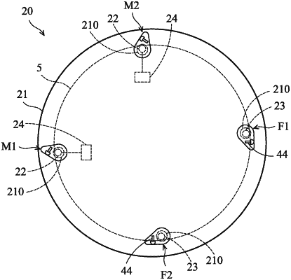
1. A semiconductor wafer cleaning apparatus, comprising:
a spin base having a through hole and a flange protruding upward from a top surface of the spin base;
a spindle extending through the through hole;
a clamping member covering the through hole and connected to the spindle, wherein the clamping member comprises a mounting part, a supporting part disposed on the mounting part, and an abutment member comprising a pillar and a ridge disposed on the supporting part, wherein the pillar is higher than the ridge; and
a first sealing ring disposed under the clamping member, wherein a top surface of the first sealing ring and a top surface of the flange are in contact with a bottom surface of the mounting part.
|