| CPC H01L 27/14616 (2013.01) [H01L 27/1463 (2013.01); H01L 27/14612 (2013.01); H01L 27/14643 (2013.01); H01L 27/14689 (2013.01); H01L 27/1464 (2013.01)] | 8 Claims |
|
1. A method for making a global shutter CMOS image sensor comprising,
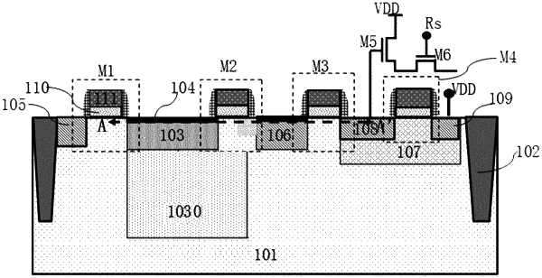
forming N rows of pixel units sequentially arranged from the front to the rear, wherein forming each pixel unit includes forming a first resetting region (105), a global shutter transistor (M1), a photodiode, a first transfer transistor (M2), a storage diffusion region (106), a second transfer transistor (M3), a floating diffusion region (108), a reset transistor (M4), and a second resetting region (109) arranged in turn;
wherein the photodiode comprises a second conducting type semiconductor layer (101) and a first conducting type first photosensitive doped region (103) formed on a top of the second conducting type semiconductor layer (101);
wherein the storage diffusion region (106) comprises a first conductivity type, and a gate structure of the first transfer transistor (M2) is formed at a top of the second conducting type semiconductor layer (101) between the first conducting type first photosensitive doped region (103) and the storage diffusion region (106);
wherein the first resetting region (105) comprises the first conductivity type, the first resetting region (105) is connected to power supply voltage, and a gate structure of the global shutter transistor (M1) is formed at the top of the second conducting type semiconductor layer (101) between the first conducting type first photosensitive doped region (103) and the first resetting region (105);
forming a pinned layer (104) comprising a second conductivity type on a surface of the first conducting type first photosensitive doped region (103);
forming a gate structure of the second transfer transistor (M3) at the top of the second conducting type semiconductor layer (101) between the floating diffusion region (108) and the storage diffusion region (106);
forming a gate structure of the reset transistor (M4) between the floating diffusion region (108) and the second resetting region (109);
the second resetting region (109) comprising the first conductivity type, and the second resetting region (109) is connected to the power supply voltage;
wherein the floating diffusion region (108) and the second resetting region (109) are formed in a second conducting type well (107);
wherein a dopant concentration of the first conductivity type in the storage diffusion regions (106) of a front M rows of the N rows of pixel units is less than a dopant concentration of the first conductivity type in the storage diffusion regions (106) of remaining rear N-M rows, wherein N is an integer greater than 10, and M is an integer less than or equal to N/2;
performing a first shallow layer ion implantation and a second shallow layer ion implantation to form the storage diffusion regions (106) of the N rows of pixel units;
wherein the first shallow layer ion implantation comprises implanting ions of the first conductivity type into storage diffusion regions (106) of all of the N rows of pixel units; and
wherein the second shallow layer ion implantation comprises implanting ions of the second conductivity type into storage diffusion regions (106) of only the front M rows of the N rows of pixel units.
|