US 11,854,787 B2
Advanced lithography and self-assembled devices
Richard E. Schenker, Portland, OR (US); Robert L. Bristol, Portland, OR (US); Kevin L. Lin, Beaverton, OR (US); Florian Gstrein, Portland, OR (US); James M. Blackwell, Portland, OR (US); Marie Krysak, Portland, OR (US); Manish Chandhok, Beaverton, OR (US); Paul A. Nyhus, Portland, OR (US); Charles H. Wallace, Portland, OR (US); Curtis W. Ward, Hillsboro, OR (US); Swaminathan Sivakumar, Beaverton, OR (US); and Elliot N. Tan, Portland, OR (US)
Assigned to Intel Corporation, Santa Clara, CA (US)
Filed by Intel Corporation, Santa Clara, CA (US)
Filed on May 2, 2022, as Appl. No. 17/735,006.
Application 17/735,006 is a continuation of application No. 17/110,215, filed on Dec. 2, 2020, granted, now 11,373,950.
Application 17/110,215 is a continuation of application No. 16/346,873, granted, now 10,892,223, issued on Jan. 12, 2021, previously published as PCT/US2016/068586, filed on Dec. 23, 2016.
Prior Publication US 2022/0262722 A1, Aug. 18, 2022
This patent is subject to a terminal disclaimer.
Int. Cl. H01L 23/528 (2006.01); H01L 23/522 (2006.01); H01L 23/532 (2006.01); H01L 27/088 (2006.01); H01L 29/78 (2006.01)
CPC H01L 23/528 (2013.01) [H01L 23/5226 (2013.01); H01L 23/5329 (2013.01); H01L 23/53238 (2013.01); H01L 27/0886 (2013.01); H01L 29/7848 (2013.01)] 19 Claims
OG exemplary drawing
 
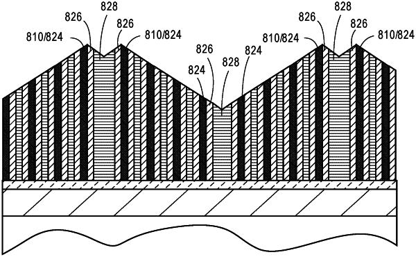
14. A target structure for fabricating an integrated circuit structure, the target structure comprising:
a first set of spacers above a hardmask layer above a substrate, the first set of spacers having a first material composition;
a second set of spacers along outer sidewalls of each of the first set of spacers, the second set of spacers having a second material composition different than the first material composition;
a third set of spacers along inner sidewalls of each of the first set of spacers, the third set of spacers having the second material composition; and
a final feature in an opening between adjacent pairs of spacers of the third set of spacers.