| CPC H01J 43/246 (2013.01) [H01J 49/025 (2013.01)] | 9 Claims |
|
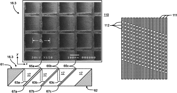
1. A metal-channel conversion dynode comprising:
a wafer comprising a first face and a second face parallel to the first face, the wafer having a thickness less than 1000 μm and comprising either tungsten, molybdenum, or a tungsten or molybdenum alloy having chemical purity of 90-99%; and
a plurality of channels passing through the wafer from the first face to the second face at an angle to a plane of the first face and a plane of the second face,
wherein no direct line of sight exists through any channel in the plurality of channels of the wafer along a sightline that is normal to the first and second faces.
|