| CPC G11C 5/148 (2013.01) | 20 Claims |
|
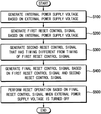
1. A method of resetting a storage device including a buffer memory and a nonvolatile memory, the method comprising:
generating an internal power supply voltage based on an external power supply voltage;
generating a first reset control signal based on a level of the internal power supply voltage;
generating a second reset control signal with a timing different from that of the first reset control signal;
generating a final reset control signal based on the first reset control signal and the second reset control signal, the final reset control signal being activated or deactivated with a timing different from those of the first reset control signal and the second reset control signal; and
performing a reset operation based on the final reset control signal when the external power supply voltage is turned off,
wherein the performing of the reset operation includes storing data stored in the buffer memory included in the storage device into the nonvolatile memory included in the storage device.
|