| CPC G11C 29/10 (2013.01) [G06F 9/30101 (2013.01); G06F 11/221 (2013.01); G11C 29/14 (2013.01)] | 20 Claims |
|
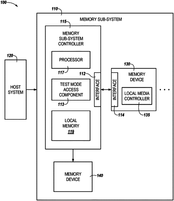
1. A system, comprising:
a memory device; and
a processing device, the processing device configured to communicate with the memory device via an interface; and
wherein the processing device is further configured to control the interface to cause the interface to:
receive, during a non-test mode, a first set of signals to cause the interface to provide a signal compliant with a particular interface protocol; and
receive, during a test mode, a second set of signals to cause the interface to provide, in response to receipt of the second set of signals, a signal non-compliant with the particular interface protocol to the memory device.
|