| CPC G11C 16/10 (2013.01) [H01L 29/6656 (2013.01); H01L 29/7841 (2013.01); H10B 41/35 (2023.02); G11C 16/04 (2013.01)] | 20 Claims |
|
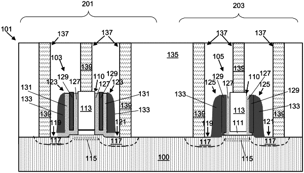
1. A memory device comprising:
a substrate; and
a plurality of transistor devices on the substrate, including at least one transistor device located in a memory region of the memory device and at least one transistor device located in a logic region of the memory device, wherein each transistor device of the plurality of transistor devices comprises:
a source;
a drain;
a channel extending between the source and the drain;
a gate structure over the channel; and
at least one sidewall spacer located on a side surface of the gate structure, and wherein each sidewall spacer of the at least one transistor device in the memory region of the memory device comprises a first oxide layer over the side surface of the gate structure, a first nitride layer over the first oxide layer, a second oxide layer having a thickness of at least 5 nm over the first nitride layer, and a second nitride layer over the second oxide layer.
|