US 11,854,614 B2
Electronic device and manufacturing method of electronic device
Young Sam Lee, Icheon (KR)
Assigned to SK hynix Inc., Icheon (KR)
Filed by SK hynix Inc., Icheon (KR)
Filed on May 7, 2021, as Appl. No. 17/315,194.
Application 17/315,194 is a continuation of application No. 16/903,041, filed on Jun. 16, 2020, granted, now 11,049,556.
Claims priority of application No. 10-2019-0130959 (KR), filed on Oct. 21, 2019.
Prior Publication US 2021/0264977 A1, Aug. 26, 2021
This patent is subject to a terminal disclaimer.
Int. Cl. G11C 13/00 (2006.01)
CPC G11C 13/0028 (2013.01) [G11C 13/0026 (2013.01)] 15 Claims
OG exemplary drawing
 
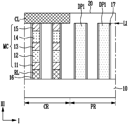
1. A method of manufacturing an electronic device including a semiconductor memory, the method comprising:
forming a cell stack in a cell region of a base;
forming a first insulating layer in a peripheral region of the base;
forming cell patterns by patterning the cell stack;
forming first dummy insulating patterns by patterning the first insulating layer;
forming liner layers on sidewalls of the cell patterns; and
forming dummy liner layers on sidewalls of the first dummy insulating patterns.