| CPC G11C 11/419 (2013.01) [G11C 7/08 (2013.01); H01L 23/5286 (2013.01); H01L 27/092 (2013.01); H10B 10/12 (2023.02); H10B 10/18 (2023.02)] | 11 Claims |
|
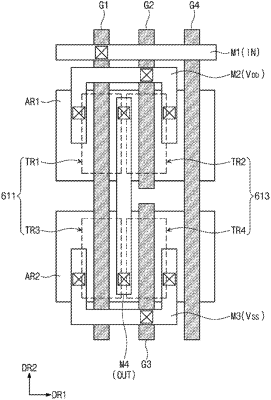
1. A semiconductor device comprising:
a first active region and a second active region extended in a first direction, the first active region and the second active region being provided in a substrate;
a first gate electrode extended in a second direction perpendicular to the first direction, wherein a first gate is extended on the first active region and the second active region;
a second gate electrode extended in the second direction on the first active region;
a third gate electrode extended in the second direction on the first active region and the second active region;
a fourth gate electrode extended in the second direction on the second active region, wherein the second gate electrode and the fourth gate electrode are on a common line of extent;
a first source/drain contact provided on the first active region at a first side of the first gate electrode;
a second source/drain contact provided on the first active region at a first side of the second gate electrode;
a third source/drain contact provided on the second active region at the first side of the first gate electrode;
a fourth source/drain contact provided on the second active region at the first side of the fourth gate electrode;
a first gate contact provided on the first gate electrode;
a second gate contact provided on the second gate electrode;
a third gate contact provided on the fourth gate electrode;
a first conductive line connected to the first gate electrode via the first gate contact;
a second conductive line which overlaps at least part of the first source/drain contact, at least part of the second source/drain contact, and at least part of the second gate contact in a plan view;
a third conductive line which overlaps at least part of the third source/drain contact, at least part of the fourth source/drain contact, and at least part of the third gate contact in the plan view; and
a fourth conductive line provided on the first active region and the second active region between a second side of the first gate electrode and a second sides of the second gate electrode and the fourth gate electrode,
wherein a first voltage is provided to the second conductive line,
wherein a second voltage is provided to the third conductive line,
wherein at least part of the third conductive line extends in the first direction, the at least part of the third conductive line intersects with the fourth gate electrode in the plan view, and
wherein the first active region and the second active region extend such that at least part of the first gate electrode, at least part of the second gate electrode, and at least part of the third gate electrode overlap with the first active region in the plan view and at least part of the first gate electrode, at least part of the third gate electrode, and at least part of the fourth gate electrode overlap with the second active region in the plan view.
|