US 11,854,599 B2
Semiconductor device, electronic component, and electronic device
Takahiko Ishizu, Kanagawa (JP); Yuto Yakubo, Kanagawa (JP); Tatsuya Onuki, Kanagawa (JP); and Shunpei Yamazaki, Tokyo (JP)
Assigned to SEMICONDUCTOR ENERGY LABORATORY CO., LTD., Kanagawa-ken (JP)
Filed by SEMICONDUCTOR ENERGY LABORATORY CO., LTD., Atsugi (JP)
Filed on Oct. 31, 2022, as Appl. No. 17/977,099.
Application 17/977,099 is a division of application No. 16/881,069, filed on May 22, 2020, abandoned.
Claims priority of application No. 2019-106982 (JP), filed on Jun. 7, 2019; application No. 2019-123905 (JP), filed on Jul. 2, 2019; and application No. 2019-155418 (JP), filed on Aug. 28, 2019.
Prior Publication US 2023/0110439 A1, Apr. 13, 2023
Int. Cl. G11C 11/40 (2006.01); G11C 11/4074 (2006.01); G11C 11/4096 (2006.01); H01L 29/786 (2006.01); H01L 27/12 (2006.01); H10B 99/00 (2023.01)
CPC G11C 11/4074 (2013.01) [G11C 11/4096 (2013.01); H01L 27/1207 (2013.01); H01L 27/1225 (2013.01); H01L 27/1255 (2013.01); H01L 29/7869 (2013.01); H01L 29/78648 (2013.01); H10B 99/00 (2023.02)] 3 Claims
OG exemplary drawing
 
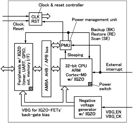
1. A system comprising:
a power management unit;
a CPU comprising a flip-flop circuit; and
a negative voltage generator,
wherein the power management unit is configured to control power gating,
wherein the flip-flop circuit is configured to back up data of the CPU in the power gating,
wherein the flip-flop circuit comprises a transistor including an oxide semiconductor in a semiconductor layer, and
wherein the negative voltage generator is configured to apply a negative voltage to a back gate of the transistor.