| CPC G11C 11/221 (2013.01) [H01L 21/76802 (2013.01); H01L 21/76805 (2013.01); H01L 21/76831 (2013.01); H01L 21/76895 (2013.01); H01L 23/5226 (2013.01); H01L 23/535 (2013.01); H01L 23/5381 (2013.01); H01L 23/5386 (2013.01); H01L 23/53209 (2013.01); H01L 23/53228 (2013.01); H01L 23/53242 (2013.01); H01L 23/53257 (2013.01); H01L 28/55 (2013.01); H01L 28/60 (2013.01); H01L 28/65 (2013.01); H03K 19/185 (2013.01); H10B 53/20 (2023.02); H10B 53/30 (2023.02)] | 21 Claims |
|
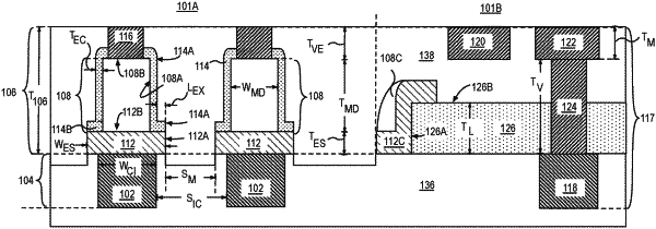
1. A device comprising:
a first region comprising:
a first conductive interconnect within a first level;
a second level above the first level, the second level comprising:
a ferroelectric memory device comprising a first height and further comprising a cylindrical shape, wherein the ferroelectric memory device is above the first conductive interconnect;
an electrode structure coupled between the ferroelectric memory device and the first conductive interconnect, the electrode structure comprising a first sidewall;
an encapsulation layer on a second sidewall of the ferroelectric memory device and on a portion of a top surface of the electrode structure, wherein an outer third sidewall of the encapsulation layer, opposite to the second sidewall is substantially aligned with the first sidewall; and
a via electrode on the ferroelectric memory device; and
a second region adjacent to the first region, the second region comprising an interconnect structure, the interconnect structure comprising:
a second conductive interconnect within the first level;
an etch stop layer comprising a dielectric material within the second level;
a metal line above the etch stop layer, wherein the metal line is within the second level; and
a via structure coupling the metal line with the second conductive interconnect, wherein the via structure is within the second level.
|
|
18. A device comprising:
a first region comprising:
a first conductive interconnect within a first level;
a second level above the first level, the second level comprising:
a ferroelectric memory device comprising a first height and further comprising a cylindrical shape, the ferroelectric memory device above the first conductive interconnect;
an electrode structure coupled between the ferroelectric memory device and the first conductive interconnect, the electrode structure comprising a first sidewall and a first vertical thickness; and
an encapsulation layer on a second sidewall of the ferroelectric memory device and on a portion of a top surface of the electrode structure, wherein an outer third sidewall of the encapsulation layer opposite to the second sidewall is substantially aligned with the first sidewall; and
a via electrode on the ferroelectric memory device; and
a second region adjacent to the first region, the second region comprising an interconnect structure, the interconnect structure comprising:
a second conductive interconnect within the first level;
an etch stop layer comprising a dielectric material and a second vertical thickness within the second level, wherein the first vertical thickness is less than the second vertical thickness;
a metal line above the etch stop layer, wherein the metal line is within the second level; and
a via structure coupling the metal line with the second conductive interconnect, wherein the via structure is within the second level.
|
|
19. A system comprising:
a processor;
a communication interface communicatively coupled to the processor; and
a memory coupled to the processor, wherein the memory comprises bit-cells, wherein one of the bit-cells includes:
a first region comprising:
a first conductive interconnect within a first level;
a second level above the first level, the second level comprising
a ferroelectric memory device comprising a first height and further comprising a cylindrical shape, the ferroelectric memory device above the first conductive interconnect;
an electrode structure coupled between the ferroelectric memory device and the first conductive interconnect, the electrode structure comprising a first sidewall;
an encapsulation layer on a second sidewall of the ferroelectric memory device and on a portion of a top surface of the electrode structure, wherein an outer third sidewall of the encapsulation layer, opposite to the second sidewall is substantially aligned with the first sidewall; and
a via electrode on the ferroelectric memory device; and
a second region adjacent to the first region, the second region comprising an interconnect structure, the interconnect structure comprising:
a second conductive interconnect within the first level;
an etch stop layer comprising a dielectric material within the second level;
a metal line above the etch stop layer, wherein the metal line is within the second level; and
a via structure coupling the metal line with the second conductive interconnect, wherein the via structure is within the second level.
|