| CPC G11C 11/1673 (2013.01) [G11C 11/161 (2013.01); G11C 11/1659 (2013.01); G11C 11/1675 (2013.01); H10N 50/80 (2023.02)] | 20 Claims |
|
1. An apparatus, comprising:
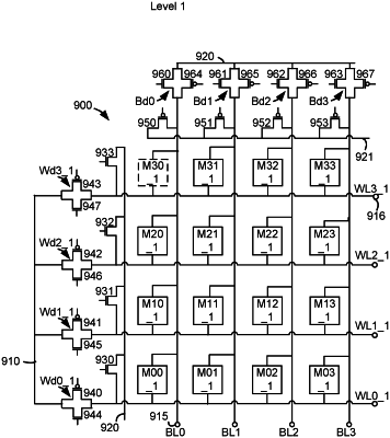
a control circuit configured to connect to a cross-point memory array, the cross-point memory array comprising a memory cell arranged between a first conductive line and a second conductive line, and a first transistor pair comprising a pMOSFET in parallel with an nMOSFET and connected to the first conductive line, the memory cell comprising a storage element in series with a threshold switching selector;
the control circuit, to select the memory cell for a read operation, is configured to pull up a voltage of the first conductive line with the pMOSFET in a conductive state while the nMOSFET is in a non-conductive state; and
the control circuit is configured to subsequently, in the read operation, read the memory cell while the nMOSFET is in a conductive state.
|