| CPC G11B 5/315 (2013.01) [G11B 5/1278 (2013.01); G11B 5/235 (2013.01); G11B 5/3116 (2013.01); G11B 5/3133 (2013.01); G11B 5/3143 (2013.01); G11B 5/3146 (2013.01); G11B 5/012 (2013.01); G11B 5/02 (2013.01); G11B 5/11 (2013.01); G11B 2005/0024 (2013.01)] | 20 Claims |
|
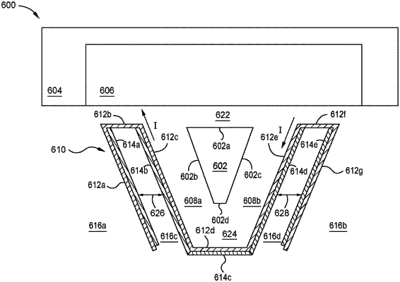
1. A magnetic recording device, comprising:
a main pole having a first surface adjacent to a trailing gap, a second surface adjacent to the first surface, a third surface opposite the second surface, and a fourth surface adjacent to a leading gap;
a trailing shield disposed adjacent to the trailing gap;
side gaps disposed below the trailing shield and surrounding the second and third surfaces of the main pole; and
a side shield surrounding the second surface, the third surface, and the fourth surface of the main pole, the side shield comprising a first layer in contact with the side gaps and a second layer in contact with the first layer,
wherein the side shield is spaced from the trailing shield and the main pole,
wherein the first layer comprises a first portion, a second portion, a third portion, a fourth portion, a fifth portion, a sixth portion, and a seventh portion,
wherein the second layer comprises a first portion, a second portion, a third portion, a fourth portion, and a fifth portion,
wherein the fourth portion of the second layer and the fifth portion of the second layer are disposed between the fifth portion of the first layer and the seventh portion of the first layer, and
wherein the fourth portion of the second layer and the fifth portion of the second layer are spaced apart by a distance of between about 15 nm and about 25 nm by an insulating material.
|