| CPC G09G 3/3258 (2013.01) [G09G 3/3266 (2013.01); G09G 3/3291 (2013.01); G09G 2300/0852 (2013.01)] | 20 Claims |
|
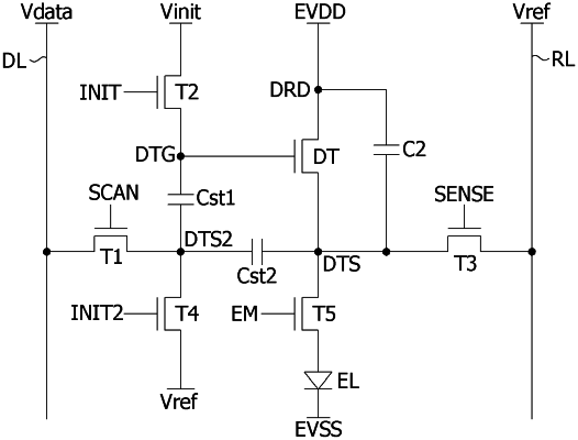
1. A pixel circuit comprising:
a driving element including a first electrode connected to a first node to which a pixel driving voltage is applied, a gate electrode connected to a second node, and a second electrode connected to a third node, and configured to supply a current to a light emitting element;
a first switch element configured to supply a data voltage of pixel data to a fourth node in response to a scan pulse;
a second switch element configured to supply an initialization voltage to the second node in response to a first initialization pulse;
a third switch element configured to supply a reference voltage lower than the initialization voltage to the third node in response to a sensing pulse;
a fourth switch element configured to supply the reference voltage to the fourth node in response to a second initialization pulse;
a fifth switch element configured to connect the third node to an anode electrode of the light emitting element in response to an emission control pulse;
a first capacitor connected between the second node and the fourth node;
a second capacitor connected between the third node and the fourth node; and
a third capacitor connected between the first node and the third node;
wherein a driving period of the pixel circuit includes an initialization step, a sensing step, a first transmission step, a data writing step, a second transmission step, a boosting step, and a light emission step;
wherein in the first transmission step, the second initialization pulse is generated as the gate-on voltage, and the first initialization pulse, the sensing pulse, the scan pulse, and the emission control pulse are generated as the gate-off voltage;
wherein in the data writing step, the scan pulse is generated as the gate-on voltage synchronized with the data voltage, and the first initialization pulse, the sensing pulse, the second initialization pulse, and the emission control pulse are generated as the gate-off voltage;
wherein in the second transmission step, the sensing pulse is generated as the gate-on voltage, and the first initialization pulse, the second initialization pulse, the scan pulse, and the emission control pulse are generated as the gate-off voltage;
wherein each of the first, second, third, fourth and fifth switch elements is turned on in response to the gate-on voltage and is turned off in response to the gate-off voltage.
|