| CPC G09G 3/325 (2013.01) [G09G 3/3291 (2013.01); G09G 2320/0233 (2013.01); G09G 2330/021 (2013.01)] | 19 Claims |
|
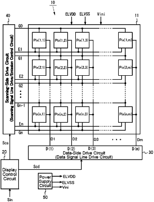
1. A pixel circuit provided to correspond to any one of a plurality of data signal lines and correspond to any one of a plurality of scanning signal lines intersecting the plurality of data signal lines in a display device including a display portion in which the plurality of data signal lines and the plurality of scanning signal lines are arranged, the pixel circuit being driven periodically with a predetermined period, including a data write period and a display period, as one cycle, the pixel circuit comprising:
a display element driven by a current;
a holding capacitor;
first and second drive transistors each configured to supply a current corresponding to a holding voltage of the holding capacitor to the display element during the display period;
a threshold compensation switching element that is connected between a control terminal and a first conduction terminal of the first drive transistor and is turned on during the data write period to set the first drive transistor in a diode connection mode; and
first and second emission control switching elements; wherein
the pixel circuit is configured such that during the data write period, by supply of a voltage of a corresponding data signal line to the holding capacitor via the first drive transistor in the diode connection mode, a data voltage corrected so as to compensate for a threshold voltage of the first drive transistor is written to the holding capacitor, and such that during the display period, a current flowing through the first drive transistor based on the corrected data voltage and a current flowing through the second drive transistor based on the corrected data voltage are supplied to the display element as drive currents;
the first conduction terminal of the first drive transistor is connected to the display element via the first emission control switching element;
a first conduction terminal of the second drive transistor is connected to the display element via the second emission control switching element; and
control terminals of the first and second drive transistors are connected to each other and are connected to the holding capacitor.
|