| CPC G09G 3/3233 (2013.01) [G09G 3/2022 (2013.01); G09G 3/3266 (2013.01); G09G 3/3291 (2013.01); G09G 3/3648 (2013.01); G09G 5/005 (2013.01); G09G 5/395 (2013.01); G09G 2300/0443 (2013.01); G09G 2300/0804 (2013.01); G09G 2300/0814 (2013.01); G09G 2300/0819 (2013.01); G09G 2300/0842 (2013.01); G09G 2300/0861 (2013.01); G09G 2310/0216 (2013.01); G09G 2310/0262 (2013.01); G09G 2310/0286 (2013.01); G09G 2310/0297 (2013.01); G09G 2310/067 (2013.01); G09G 2310/08 (2013.01); G09G 2320/0233 (2013.01); G09G 2320/045 (2013.01); G09G 2330/028 (2013.01); G09G 2360/02 (2013.01); G09G 2360/123 (2013.01); G09G 2370/04 (2013.01)] | 18 Claims |
|
1. An active array organic light emitting diode (AMOLED) display, comprising:
an array of OLEDs divided into k groups of OLEDs, where k is an integer larger than 1, the k groups of OLEDs being organized into either rows or columns;
a plurality of pixel circuits connected to the array of OLEDs, wherein each of the plurality of pixel circuits is configured to sequentially drive k OLEDs from each of the k groups of OLEDs;
a light emitting driver connected to the plurality of pixel circuits and configured to cause each of the k groups of OLEDs to sequentially emit light in a respective one of k sub-frame periods within a frame period; and
a gate scanning driver connected to the plurality of pixel circuits and configured to provide a scan signal to sequentially scan each of the k groups of OLEDs in the respective sub-frame period within the frame period, wherein:
each of the plurality of pixel circuits comprises:
a capacitor,
a single light emitting control transistor comprising a gate electrode connected to a light emitting control signal provided by the light emitting driver, a source electrode connected to a supply voltage signal, and a drain electrode connected to a driving transistor,
the driving transistor comprising a gate electrode connected to one electrode of the capacitor, a source electrode connected to the drain electrode of the single light emitting control transistor, and a drain electrode connected to k light emitting transistors of the k OLEDs, and
the k light emitting transistors, each of which comprising a gate electrode connected to a respective one of k light emitting signals provided by the light emitting driver, a source electrode connected to the drain electrode of the driving transistor, and a drain electrode connected to a respective one of the k OLEDs;
the light emitting control signal is configured to turn off the single light emitting control transistor during a charging period of each of the k sub-frame periods and turn on the single light emitting control transistor during each of the k sub-frame periods after a respective charging period, the light emitting control signal is configured to repeatedly turn off and on the single light emitting control transistor k times during the frame period;
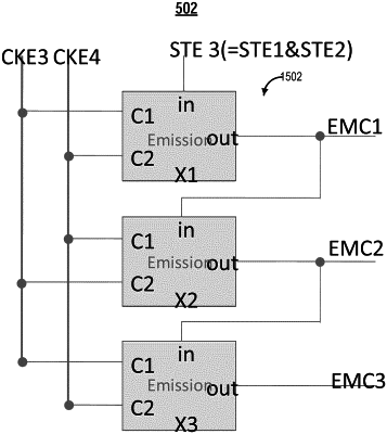
the light emitting driver comprises a light emitting circuit and a light emitting control circuit, the light emitting circuit comprises k first shift registers configured to provide k light emitting signals in response to k first enable signals, and the light emitting control circuit comprises a second shift register configured to provide the light emitting control signal in response to a second enable signal that is a logical disjunction of the k first enable signals;
each of the k light emitting signals is configured to coordinate with the light emitting control signal to turn on the respective light emitting transistor during a respective one of k sub-frame periods within the frame period to cause the respective OLED to emit light;
the light emitting control signal is separate from each of the k light emitting signals and the scan signal;
a plurality of scan lines operatively coupled to the array of OLEDs, wherein each of the plurality of scan lines is shared by k rows of OLEDs from each of the k groups of OLEDs when the k groups of OLEDs are organized into rows; and
a plurality of data lines operatively coupled to the array of OLEDs, wherein each of the plurality of data lines is shared by k columns of OLEDs from each of the k groups of OLEDs when the k groups of OLEDs are organized into columns.
|