| CPC G09G 3/006 (2013.01) [G01N 21/8851 (2013.01); G01N 21/95607 (2013.01); H10K 71/00 (2023.02)] | 19 Claims |
|
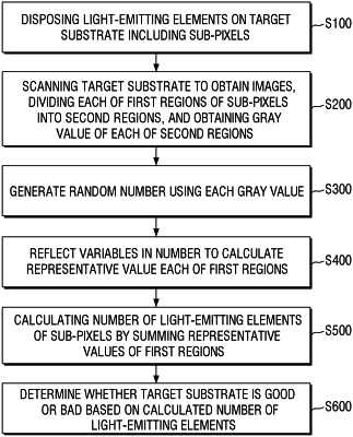
1. A method for inspecting a display device, the method comprising:
preparing a target substrate comprising sub-pixels, which includes disposing light-emitting elements on the target substrate, wherein disposing includes
forming a first electrode layer and a second electrode layer on the target substrate;
spraying an ink containing the light-emitting elements dispersed in a solvent onto the target substrate; and
generating an electric field over the target substrate to align the light-emitting elements;
dividing each of a plurality of first regions of the sub-pixels into a plurality of second regions;
obtaining a gray value of each of the plurality of second regions;
generating a random number using the gray value;
calculating a representative value of each of the plurality of first regions by reflecting variables in the random number;
summing the representative values of the plurality of first regions to calculate a number of light-emitting elements of the sub-pixels; and
if the number of light-emitting elements of the sub-pixels more than a predetermined value, performing subsequent processing on the display device.
|