| CPC G06V 40/1324 (2022.01) [A61B 5/1172 (2013.01); G06F 21/32 (2013.01); G06V 40/1341 (2022.01); G06V 40/1365 (2022.01); G06V 40/145 (2022.01)] | 8 Claims |
|
1. A detection device comprising:
a plurality of optical sensors arranged in a detection area;
a light source configured to emit light that is emitted to an object to be detected and is detected by the optical sensors; and
a processor configured to perform processing based on outputs from the optical sensors,
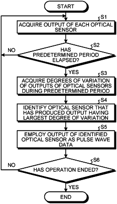
wherein the processor is configured to determine, based on the outputs of the respective optical sensors obtained at a cycle of a predetermined period, an optical sensor to be employed from among the optical sensors,
wherein the detection area comprises a plurality of group areas,
wherein each of the group areas comprises the optical sensors each disposed in a partial detection area, and
wherein the processor is configured to employ an output of the group area including the partial detection area in which the optical sensor that has produced an output having a largest degree of variation during the predetermined period.
|