| CPC G06V 40/1318 (2022.01) | 22 Claims |
|
1. An electronic device, comprising:
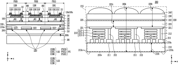
a display panel including a light emitter, and
a biometric sensor stacked with the display panel in a vertical direction extending perpendicular to an outer surface of the display panel, the biometric sensor being configured to detect light emitted from the light emitter of the display panel and reflected by a recognition target that is external to the electronic device,
wherein the biometric sensor includes
a silicon substrate including a charge storage, and
a photoelectric conversion element on the silicon substrate and electrically coupled to the charge storage of the silicon substrate, such that the photoelectric conversion element is between the silicon substrate and the light emitter, the photoelectric conversion element including a photoelectric conversion layer having wavelength selectivity configured to absorb light in a visible wavelength spectrum,
wherein the biometric sensor does not comprise any color filter,
wherein the photoelectric conversion element further includes
a lower electrode and an upper electrode facing each other,
a buffer layer that is between the lower electrode and the photoelectric conversion layer or between the upper electrode and the photoelectric conversion layer,
a first encapsulation layer that is on the upper electrode, and
a lens on the first encapsulation layer,
wherein the photoelectric conversion layer is between the lower electrode and the upper electrode,
wherein at least one of the lower electrode or the upper electrode is a light-transmitting electrode, and
wherein the electronic device further includes a second encapsulation layer between the display panel and the lens of the biometric sensor, the second encapsulation layer being on both the lens and the silicon substrate, wherein the display panel has a lower surface that is coupled to the second encapsulation layer based on at least one of
the lower surface being in direct contact with the second encapsulation layer, or
the lower surface being attached to the second encapsulation layer by an adhesive or a fixing member.
|