| CPC G06N 3/0675 (2013.01) [G02B 6/425 (2013.01); G02B 6/4206 (2013.01); G02F 1/212 (2021.01); G02F 1/2257 (2013.01)] | 12 Claims |
|
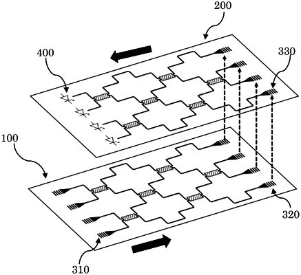
1. A method for manufacturing a photonic semiconductor device, comprising:
dividing a photonic neural network which is a photonic network configured for the photonic semiconductor device into a plurality of sub-photonic networks;
forming the plurality of sub-photonic networks on a plurality of photonic chips;
connecting the plurality of sub-photonic networks on the plurality of photonic chips through a coupler to obtain the photonic semiconductor device carrying the photonic neural network, wherein the coupler is configured to couple light from one photonic chip to another photonic chip.
|