| CPC G06F 30/34 (2020.01) [G06F 11/261 (2013.01); G06F 11/3652 (2013.01); G06F 21/76 (2013.01)] | 16 Claims |

|
1. A method for emulating a design of an electronic circuit, the method comprising:
executing a netlist of a set of field-programmable gate array (FPGA) overlays for a design of an electronic circuit;
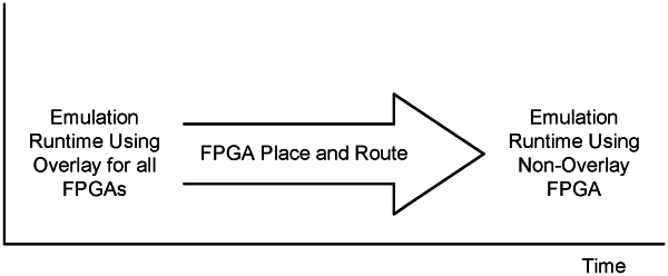
executing through an emulator a first place-and-route operation for a first portion of the netlist having a critical timing path to substitute a first set of placed and routed FPGAs into a first set of logic elements of the design of the electronic circuit to generate a first updated netlist corresponding to a first updated design of the electronic circuit;
executing through the emulator the first updated netlist and concurrently executing a second place-and-route operation for a second portion of the netlist separate from the critical timing path to substitute a second set of placed and routed FPGAs into a second set of logic elements of the electronic circuit to generate a second updated netlist;
interconnecting the first set of placed and routed FPGAs and the second set of placed and routed FPGAs to implement a second updated design of the electronic circuit; and
executing through the emulator the second updated design of the electronic circuit using the interconnected first placed and routed FPGAs and FPGAs the second placed and routed FPGAs.
|