| CPC G06F 3/0659 (2013.01) [G06F 3/0604 (2013.01); G06F 3/0656 (2013.01); G06F 3/0673 (2013.01); G11C 13/0069 (2013.01); G11C 2213/30 (2013.01)] | 20 Claims |
|
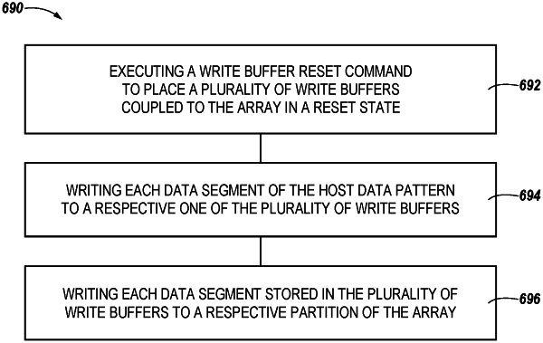
1. A method, comprising:
placing, responsive to a write buffer reset command received to write a host data pattern to a managed unit of an array of resistance variable memory cells, binary data states of storage locations of a first write buffer of Y write buffers coupled to the array in a same binary data state, wherein Y is a positive integer greater than 1;
placing, responsive to the same write buffer reset command, binary data states of storage locations of a second write buffer of the Y write buffers in a same binary data state; and
writing Y data segments of the host data pattern to the Y write buffers to execute a set of Y write commands subsequent to the write buffer reset command.
|