| CPC G06F 3/0614 (2013.01) [G06F 3/064 (2013.01); G06F 3/0631 (2013.01); G06F 3/0659 (2013.01); G06F 3/0679 (2013.01); G06F 11/3037 (2013.01); G06F 11/3058 (2013.01)] | 20 Claims |
|
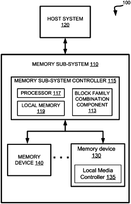
1. A system comprising:
a memory device; and
a processing device, operatively coupled to the memory device, the processing device to:
identify a first temperature level of a first set of memory blocks associated with the memory device;
identify a second temperature level of a second set of memory blocks associated with the memory device;
determine that a condition is satisfied based on a comparison of the first temperature level, the second temperature level, and an adjustable threshold level; and
in response to the condition being satisfied, combine the first set of memory blocks and the second set of memory blocks to generate a combined set of memory blocks.
|