| CPC G06F 3/0446 (2019.05) [G06F 3/045 (2013.01); G06F 3/0416 (2013.01); G06F 3/0443 (2019.05); G06F 2203/04107 (2013.01); G06F 2203/04111 (2013.01); G06F 2203/04112 (2013.01)] | 15 Claims |
|
1. An electronic device comprising:
a base substrate defining an active area configured to display an image, and a hole area and a non-active area adjacent to the active area;
a display element to display the image, the display element being on the base substrate;
an encapsulation layer comprising inorganic layers, and an organic layer between the inorganic layers and covering the display element; and
a sensing layer comprising first sensing electrodes and second sensing electrodes insulated from each other, the sensing layer being on the encapsulation layer;
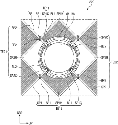
wherein an opening penetrates through the base substrate, the encapsulation layer, and the sensing layer, the opening overlapping the hole area,
wherein the second sensing electrodes comprise adjacent second sensing electrodes crossing the opening, each of the adjacent second sensing electrodes comprising:
a main pattern;
an adjacent pattern adjacent to the opening and having an area smaller than that of the main pattern;
a compensation pattern in the hole area and surrounding at least a portion of the opening; and
a connection line connecting the adjacent pattern and the compensation pattern.
|